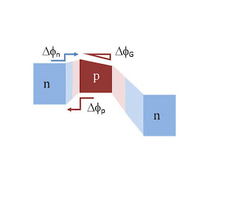
Due to the need to manufacture HBT devices with extremely high-doped thin base layers, molecular beam epitaxy is principally employed. In addition to base, emitter and collector layers, highly doped layers are deposited on either side of collector and emitter to facilitate an ohmic contact, which are placed on the contact layers after exposure by photolithography and etching. The contact layer underneath the collector is, named subcollector, is an active part of the transistor.
Other techniques are used depending on the material system. IBM and others use UHV CVD for SiGe; other techniques used include MOVPE for III-V systems.

No hay comentarios:
Publicar un comentario